深圳市誉辉天成电子有限公司
- 品质保障
- 质量第一
- 品类齐全
元器件产品
COMPONENT PRODUCTSIC芯片(101806)
逻辑IC(14)
射频IC(2)
时钟IC(6)
其他IC(1267)
处理器MPU(1)
DC-DC(3)
LED驱动IC(9)
稳压IC(63)
充电管理IC(9)
其他电源IC(73)
贴片/片式/SMD二极管(38)
整流二极管(12)
整流二极管模块(2)
稳压二极管(1)
瞬态(变)抑制二极管(5)
肖特基二极管(2)
激光(光电)二极管(1)
齐纳/雪崩二极管(3)
TVP管(2)
二极管芯片(管芯)(1)
其他二极管(38)
三极管芯片(管芯)(1)
MOSFET(280)
结型场效应管(3)
IGBT模块(4)
单向可控硅(晶闸管)(1)
可控硅(晶闸管)模块(2)
单片机产品/套件(2)
单片机MCU(7)
铝电解电容(5)
钽电解电容(6)
高压电容(1)
陶瓷电容(2)
其他电容(2)
贴片/片式电阻(1)
其他电感器(5)
模块电源/电源模块(54)
线性电源(1)
直流稳压电源(1)
其他类型电源(5)
其他晶振器件(2)
矩形/重载连接器(2)
板对板连接器(1)
电源连接器(1)
IC连接器(1)
插头(座)(1)
其他连接器(3)
霍尔传感器(2)
温(湿)度传感器(14)
其他传感器(3)
其它保险丝(1)
固态继电器(3)
通信继电器(1)
其它逆变器(3)
放大器(83)
光电光耦合器(光耦)(1)
其他光电子、激光器件(4)
LED器件(1)
LED芯片及外延(5)
其它电子原辅材料(1)
滤波器(4)
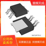
产品简介:
The TLC271 operational amplifier combines a wide range of input offset voltage grades with low offset voltage drift and high input impedance. In addition, the TLC271 offers a bias-select mode that allows the user to select the best combination of power dissipation and ac performance for a particular application. These devices use Texas Instruments silicon-gate LinCMOSTM technology, which provides offset voltage stability far exceeding the stability available with conventional metal-gate processes.
Using the bias-select option, these cost-effective devices can be programmed to span a wide range of applications that previously required BiFET, NFET, or bipolar technology. Three offset voltage grades are available (C-suffix and I-suffix types), ranging from the low-cost TLC271 (10 mV) to the TLC271B (2 mV) low-offset version. The extremely high input impedance and low bias currents, in conjunction with good common-mode rejection and supply voltage rejection, make these devices a good choice for new state-of-the-art designs as well as for upgrading existing designs.
In general, many features associated with bipolar technology are available in LinCMOSTM operational amplifiers, without the power penalties of bipolar technology. General applications such as transducer interfacing, analog calculations, amplifier blocks, active filters, and signal buffering are all easily designed with the TLC271. The devices also exhibit low-voltage single-supply operation, making them ideally suited for remote and inaccessible battery-powered applications. The common-mode input voltage range includes the negative rail.
A wide range of packaging options is available, including small-outline and chip-carrier versions for high-density system applications.
The device inputs and output are designed to withstand -100-mA surge currents without sustaining latch-up.
The TLC271 incorporates internal ESD-protection circuits that prevent functional failures at voltages up to 2000 V as tested under MIL-STD-883C, Method 3015.2; however, care should be exercised in handling these devices as exposure to ESD may result in the degradation of the device parametric performance.
The C-suffix devices are characterized for operation from 0°C to 70°C. The I-suffix devices are characterized for operation from -40°C to 85°C. The M-suffix devices are characterized for operation over the full military temperature range of -55°C to
特征介绍:
 Hz\ Typically at
 Typ
Typ
技术参数:
应用领域:

深圳市誉辉天成电子有限公司
联系人:龙婷
传真:0755-82534548
地址:广东省深圳市福田区赛格科技园4栋中5楼505
电话:18028704788
手机:18720511991/13410894495/18720511991/ 15919489657
QQ: 


 询价
询价